Written in 1998 By James A. Forster, Kiyokazu Ikeya, Masao Tohyama and Sal P. Rizzo
Sensata Technologies (formerly Texas Instruments), Mansfield, MA
Abstract
The move from Ball Grid Array to Fine Pitch BGA is being driven by the need to reduce package size. In addition the increased number of I/O associated with increased functionality creates additional pressure to reduce the pitch of the array. The BGA package maximizes the number of I/O within a given area, and the need for smaller and smaller footprints has driven the development of packages with pitches less than 1.0 mm. The development of the Chip Scale Package in the last three years is a testament to the interest and need for ever smaller packages. The supporting "Infrastructure", necessary to allow commercialization of the technology, is often the gating item for the board acceptance of any new package. An important part of that infrastructure is burn-in test sockets.
Fine Pitch BGA packages incorporate pitches less than 1.0 mm which presents a number of challenges to the printed wiring board industry and burn-in socket designers. Contacting solder balls at temperatures of 125°C, without touching the bottom of the ball or leaving a significant witness impression on the ball, is a particular difficulty. Designing and manufacturing components for a socket to contact and hold a package, within the space available between the solder balls, adds to the challenge. This paper will describe some of the methods currently being used to contact solder balls. One solution for pitches between 1.0 mm and 0.75mm, that uses a dual beam pinch contact, will be described and utilized to illustrate how these challenges were overcome.
Today there are flash memory devices packaged with a pitch of 0.65 mm and DSPs with 100+ I/O in 0.5 mm FP–BGA packages. A cost–effective solution for burn-in sockets must be developed for these devices. Some of these concepts will be discussed.
Introduction
While the "Electronics Age" has come and gone and we are now in the "Information Age" it is the electronics and communications industries which provide the engine and power to enable the delivery of all the electronic information. Cell/digital phones, pagers, Computers—desktops, laptops; palmtops and Personal Digital Assistants all deliver information via a variety of techniques including the Internet and CD–ROMs.
The challenge from the invention of the transistor and integrated circuit has been to put more power and functionality into a smaller package while making the package easy to handle and interface with the outside world. This has resulted in an alphabet soup of packages which includes, DIP, PGA, PLCC, LCCC, QFP, TQFP and BGA to name a few.
| |
 |
| |
Figure 1: Size benefit of CSP over QFP |
The growth of the personal electronics industry, especially in Japan, has provided the incentive to reduce system size and weight and the need for development of smaller and smaller packages. All the packaging road maps show bare die however the difficulties and cost of handling and test have delayed the broad acceptance of this format. As a compromise between a conventional package and a bare die recent efforts to reduce size have resulted in the development of a class of packages which are about the size of the silicon die, the so called Chip Size or Chip Scale Package (CSP).
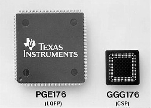
Figure 1 is a photograph comparing the size of a product packaged as a QFP and as a FP–BGA. Intel[1] has indicated that an 8–Mbit flash memory packaged as a µBGA is 80% smaller than a comparable TSOP.
The acceptance and use of chip scale packages appears to be most prevalent in Japan [2]. While there are more than 50 different CSP constructions[3], and each semiconductor company seems to have their own variety, the difficulties of handling and testing these devices has challenged the infrastructure suppliers serving back end and test. This will continue to be concern if Gil Olachea’s prediction is correct. Following Moore’s law for chip density increases Olachea[4] has proposed that:
"the number of semi–conductor packages doubles approximately every six years." This would suggest that there would be more than 120 different types of CSP by 2001.
One class of CSP which appears most favored is the Fine Pitch Ball Grid Array (FP–BGA). This is a logical development of the BGA with the pitch and ball size being reduced. FP–BGA is generally classified as a BGA with the balls on centres less than 1.0 mm and standards are either written or being prepared around pitches of 0.8, 0.75 and 0.5 mm.
This paper will focus on some of the issues facing the designer of burn-in and test sockets for FP–BGA’s and illustrate how one design for pitches of 0.75 mm and above has addressed some of challenges. burn-in sockets for pitches of 0.5 mm are available however they are considered custom and developmental; this paper will review some of the solutions currently being considered.
Design Considerations
General Commercial Issues
The requirements for burn-in sockets involve functional consideration of mechanical, electrical, thermal, reliability and re–usability and the commercial issues of cost. These requirements are subtly different than those for test. The challenge of contacting I/O on a pitch of less than 1.00 mm is identical for both types of socket however the test frequency, number of re–uses and the thermal exposure are very different. Pfaff[5] has provided an excellent review of the commercial and technical issues involved in the development of sockets for CSP’s.
Figure 2 is from Pfaff’s paper and summarizes the key requirements and differences between test and burn-in.
Characteristic |
Test Socket |
Burn-in Socket |
Insertions |
100K to 1Million+ |
10,000 typical |
Electrical |
High frequency: GHz range
Low Inductance: <4nH |
Low frequency: <250 MHz
Higher inductance: 5 to 13 nH |
Production Method |
Machined |
Injection molding |
Contact Technology |
Pogo, Particle Interconnect, Fuzz Button |
Stamped or Formed Be–Cu Spring Contact |
Device Insertion Time |
3 seconds to 5 minutes |
8 hours to 1000 hours |
DUT Board Type |
Surface Mount |
Through Hole |
Typical Order Size |
1 to 50 sockets |
300 to 20K sockets |
Typical Cost (each) |
$1,000–$6,000 |
$4–$200 |
Market Size |
$80M–$100M |
$250M–$300M |
Figure 2: Comparison of requirements for sockets for test and for burn-in (from Pfaff[5]) |
Volume is the key to the differences in manufacturing processes used and the price difference between test and burn in sockets. During the early use and acceptance of a new package, the price of sockets for burn-in will be high and this is the case today for CSP sockets. Conventional TSOP sockets for memory devices range in price from $6 to $15 depending on specific volume and number of I/O. A socket for a 0.75 mm FP–BGA with 48 I/O ranges in price from $35 to $50 — this price is driven entirely by volume considerations. Suppliers have indicated that prices will follow the conventional learning curve/volume ramp and expect that prices of $10 to $15 will be common when volumes increase.
Some concern has been expressed[5] about the individual nature of CSP’s and the lack of a standard for the overall package outline. Implicit in this concern is that the CSP sockets will remain a custom solution and that the opportunity to reduce costs, by producing a socket which can be sold to many customers, will not be realized. This is a design consideration and will be addressed below.
The market for CSP’s is reported[6] to be about 400 million packages in 1998 growing to 2.1 billion in 2000, a CAGR of 15%. Other forecasts are not as aggressive but also indicate a significant opportunity for the growth of CSP’s with volumes between 1 and 2 billion units in 2000.[3,7,8]. While not all packages are burned–in, this growth offers a substantial opportunity and socket suppliers are working diligently to develop cost effective solutions.
Mechanical
A number of design issues must be considered in the development of a burn-in socket. These are review below and include:
-
| |
 |
| |
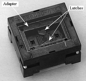
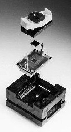
Figure 3: Open top socket for a 54 I/O µBGA flash memory device |
Device Loading
There are basically two types of socket designs; clamshell and open top. The clamshell design is favored for low volume manual load and unload. For higher volume applications a zero insertion force or open top design is preferred due to the simplicity of the device load and unload using current automated equipment.
Figure 3 is a photograph of an open top socket which has been designed for a 54 I/O µBGA memory product. The adapter which provides the location of the device and the latches which centre the package are outlined.
When the cover of the socket is depressed the contacts open and the latches move to the side. The package is dropped into the socket and is aligned by the sides of the adapter. When the cover is closed the latches guide the package and ensure that it is positioned correctly so that the contacts close on the balls.
-
| |
 |
| |
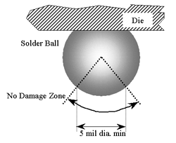
Figure 4: “No Damage Zone”, or probe "Keep–Out" area required by major CSP socket customer |
| |
| |
 |
| |
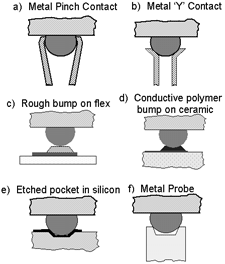
Figure 5: Schematic of some of the concepts used for contacting solder balls |
Number of Insertions
Sockets are required to be re–used multiple times and a typical design requirement is 10,000 uses or 20,000 actuations. This places requirements on the ability of the components to sustain the wear and on the stress and low cycle fatigue strength of spring elements. Many of these issues can be evaluated in the design stage using Finite Element modeling techniques and rapid prototyping to test basic concepts before investing in hard tooling.
- Contacting the Solder Ball
This is a complex issue and a number of different concepts have been proposed. Design issues include:
A. Contacting the ball without causing any damage
B. Penetrating the surface oxides
C. Keeping out of the NDZ (No Damage Zone) as shown in figure 4
A number of techniques have been proposed for contacting the balls and fall into three basic categories. Some of these do not satisfy the requirement of not touching the bottom of the solder ball:
A. Pinch style contacts which involve some kind of spring element which contacts the side of the ball
B. Probe contacts such as pogo pins and Fuzz buttons
C. Membrane contacts including conductive epoxy on ceramic, rough bumps on flex and etched pockets in silicon
Some of these are shown schematically in figure 5. For a more complete listing and description the reader should consult an excellent analysis by Crowley of the CSP market and technology.[3]
-
| |
 |
| |
Figure 6: Schematic of the tip of a pinch contact used for contacting the solder balls in a 0.75 mm socket |
| |
| |
 |
| |
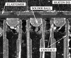
Figure 7: Cross–section through the socket showing the pinch contacts touching the solder balls |
| |
| |
 |
| |
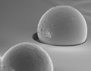
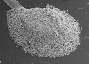
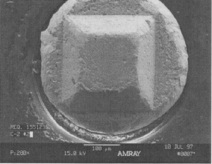
Figure 8: SEM photograph of the probe marks on a ball after burn-in at 125°C for 9 hours |
Thermal Exposure
burn-in ovens operate at a variety of different temperatures. However a typical maximum burn-in temperature is 150°C and during the life of the socket the total time at temperature can exceed 1,000 hrs. Since the contacts are loaded during burn-in the spring element is subjected to stress relaxation. One of the best alloys for spring applications is CDA-172000 which is a beryllium copper alloy. This material has been used extensively in burn-in sockets due to it’s excellent combination of formability, modulus, high yield strength, and stress relaxation performance.
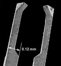
A stamped and formed contact made from beryllium copper for a 0.75 mm pitch socket is shown in figure 6. This is a state of the art metal formed part where the thickness of the sheet material is only 0.12mm (0.0047").
An advantage of the pinch style of contact is that the contact load is provided by stressed cantilever springs — there is no load applied to the surface of the package. The only vertical load on the die is through the latches which align the package in the socket. For contacts which use a pogo pin, plated bump or other kind of probe pin, a vertical load must be applied through the die. Since the die, in many CSP’s, is the package this means pressing directly on the silicon and there is an opportunity to damage the die.
By appropriate design and assembly techniques the pinch contact can satisfy the requirement not to leave a probe mark on the bottom of the ball. Figure 7 is a cross–section through the socket shown in figure 3 with a die in–place and shows a number of contacts griping the solder balls.
The grip is above the equator of the solder ball and the contact probe marks are outside the “No Damage Zone”. The position of this gripping action has the added benefit of holding the package in the socket during testing. The witness marks left on a solder ball after burn-in at 125°C for 9 hours is shown in figure 8.
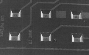
- Interface With the BIB (burn-in Board)
As shown in figure 2, the majority of burn-in boards are through hole. The standard PWB technology can easily accommodate sockets with an I/O pitch of 1.2 through 1.00 mm. However for CSP’s the pitch is less than 1.0 mm and for high I/O devices this can create problems of signal escape for the BIB manufacturer. Drilling through holes for sockets with an I/O pitch of 0.75 mm is not routine and is more costly today. No one has demonstrated a through hole technology burn-in board for sockets with a pitch of 0.5 mm.
| |
 |
| |
Figure 9: Photograph of an inter–poser used on a 48 I/0 0.75 mm CSP socket to make interfacing with the BIB easier |
To reduce or eliminate the issues of interfacing to the BIB an inter–poser can be used. This is also referred to as a fan–out board and is a small daughter card which is soldered to the base of the socket. This inter–poser provides an interface to the burn-in board at the more conventional 1.27 mm. In addition the size of the pins is increased providing greater strength and ease of handling during assembly on the BIB.
An inter–poser and socket are shown in figure 9. The robustness of the pins on the inter–poser compared to the contact tail on the socket is clear. The footprint of the inter–poser is identical to the socket so there is no penalty in BIB real estate to using the inter–poser. The height of the socket is increased by less than 2 mm or (0.080").
- Change in Package Size
A key challenge to socket suppliers will be the ability to accommodate changes in package size over the life of a product. Die shrinks are an integral part of the cost reduction programs during the life of a semi–conductor product. For conventionally packaged parts the device footprint is defined at the beginning of a program and the die shrinks are accommodated within the package and have no impact on the sockets or other test contactors. For many chip scale packages the die size defines the device footprint. As the die shrinks the overall package size will decrease and this is equivalent to a new package or device — the sockets which are in place will not be able to handle the new package without modification. The potential impact of this on infrastructure costs, given that some die will go through 2 or 3 die shrinks during the life of the product, is significant.
Socket designers at Sensata have considered this and the socket shown in figure 3 has a removable adapter, shown outlined in the figure. This adapter is a precision molded part which aligns the die to the pinch contacts and can be removed even after the sockets are installed on the burn-in board. This ability to retrofit in the field by replacing the adapter allows the end user to easily accommodate any change in the package footprint during the life of the part.
This adapter also allows the use of the same socket in a number of applications provided that the I/O footprint is identical and that the package fits within the outline capability for the socket.
| |
 |
| |
Figure 10: Photograph of Sensata’s DieMate Known Good Die Test carrier, which is being evaluated for use with 0.5 mm CSP |
| |
| |
 |
| |
Figure 11: Photograph of an epoxy pad for contacting the solder balls on FP–BGA with pitches less than 0.75mm |
| |
| |
 |
| |
Figure 12: Photograph of an epoxy pad for contacting the solder balls on FP–BGA with pitches less than 0.75mm |
| |
| |
 |
| |
Figure 13: SEM photograph of the etched Si–Pocket for contacting balls on 0.5 mm pitch |
| |
| |
 |
| |
Figure 14: SEM photograph of the solder ball after burn in using a Si–Pocket inter–poser |
The Future
The need for a cost effective solution for packages with pitches less than 0.75 mm has been identified by a number of customers. A number of techniques are available today but these are not considered cost effective and are not easily adapted to use in the installed base of high volume handling and processing equipment. In general these techniques are extensions of carriers developed for testing bare die.
Contact Pads on Flex Membranes
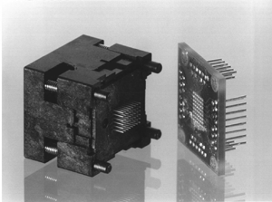
Sensata’s DieMate product with a flexible membrane manufactured by MMS is shown in
figure 10. This technology is currently being evaluated for use in CSPs.
Conductive Epoxy Bumps
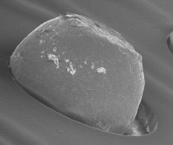
Conductive epoxy bumps on ceramic or flex can be used to contact the solder balls. The deformation on the bottom of the ball is inside the "No Deformation Zone" and is dependent on the contact load and temperature/time used.
Figure 11 is a photograph of a typical conductive epoxy contact bump. The deformation of a solder ball after burn-in is shown in
figure 12. The flattening of the bottom of the ball is clear.
Silicon Inter–Posers
Another method which has been suggested is the use of an etched silicon pocket[9] shown in
figure 13. This is another extension of a known good die carrier technique and the resultant probe mark is shown in
figure 14. Again the bottom of the ball has been deformed.
Summary
burn-in sockets for chip scale devices with pitches of 0.8 and 0.75 are commercially available today. Due to the low volumes associated with the early implementation of this package the prices for sockets are higher than for sockets for conventional packages. This is associated with the early phase of the CSP product life cycle and projections are that the prices will reduce as volume requirements approach those associated with conventional packages.
Sockets for 0.5 mm pitch packages are available however prices of $100 + are considered too high. A number of companies are reported to be working the design issues however a low cost solution has proved elusive. As the power of consumer products increases the need for a cost effective 0.5 mm socket will drive the developmental efforts. Some of the methods being considered to contact the 0.5 mm FP–BGA have been described here however a clear winner has not been identified.
Efforts at Texas Instruments and other socket companies continue to evaluate different membrane approaches and also to examine the potential for a mechanical solution. Sensata’s socket road map indicates a goal of a production–worthy socket by the end of 1998. This is a significant challenge but must be met if we are to intercept the market need and opportunity.
References
- Anonymous; “The µBGA Package: Intel’s
Latest Flash Memory Packaging Innovation”; Internet page at http://developer.intel.com/design/flcomp/packdata/ubgaback.htm.
- Goodman, T.; “CSP’s in Japanese Portable Products”, proc. Technical Conf. At Chip Scale International ’98", Vol.1, pp.49–52., pub. IPC. 1998.
- Crowley, R.T.; “Chip Scale Packaging: Technology Analysis and Market Forecast”, pub. Redpoint Research, Feb. 1998.
- Olachea, G.; “IC Packaging for the 21st Century”, Electronic Packaging & Production, pp. 57–62, Vol. 37, No. 15; pub Cahners; Nov. 97.
- Pfaff, D.; “Burn-in Socket Requirements for CSP”, proc. Technical Conf. At Chip Scale International ’98”, Vol. 2, pp.33–35., pub. IPC. 1998.
- Levine, B.; “The year of the Chip Scale package”; pp. 62–63, Electronic News, Jan. 5, 1998.
- Turlik, I.; “Chip Scale Packaging Technology Trends”, Chip Scale Review Vol. 1, No. 2, pp.30–35, pub. Tessera. July, 1997.
- Goodman, T., and Vardaman, J, “Chip Scale Packages”, pp. 72–74, Printed Circuit Fabrication, 1998.
- Anonymous; “CSP Products”; Internet page at www.bearkgd.com/cspInserts.htm
